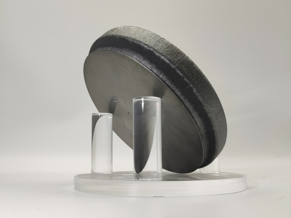
When it comes to commercial silicon carbide substrates, the industry's attention is almost entirely focused on 4H-SiC. Thanks to its high breakdown field and wide bandgap, 4H-SiC has become the core substrate material for automotive inverters, photovoltaic inverters, and charging-pile modules. Yet few people systematically examine another member of the silicon carbide family with strong product potential: 3C-SiC (cubic silicon carbide). It is the only cubic polytype of SiC, with an ABCABC atomic stacking sequence that forms a zinc-blende crystal structure. In terms of electrical performance, manufacturing cost, and large-diameter wafer scalability, 3C-SiC occupies a distinctive position and is a substrate solution that cannot be overlooked for medium-/low-voltage power devices, high-temperature sensors, and MEMS.

Fig. 1 Channel mobility comparison between 3C-SiC and 4H-SiC.
1. Key Electrical Parameters: Where 3C-SiC's Differentiation Lies
The paper systematically compares the core electrical parameters of four materials: Si, 3C-SiC, 6H-SiC, and 4H-SiC. From a substrate product perspective, 3C-SiC does not outperform 4H-SiC on every dimension; however, in the two dimensions that matter most to MOS devices—electron mobility and SiC/SiO2 interface quality—it enjoys inherent advantages.
| Parameter |
Si |
3C-SiC |
6H-SiC |
4H-SiC |
| Bandgap Eg (eV) |
1.12 |
2.35 |
3.08 |
3.28 |
| Breakdown field (MV/cm) |
0.3 |
1.5 |
2.2 |
2.3 |
| Electron mobility μₙ (cm²/V·s) |
1350 |
900 |
370 |
800 |
| Hole mobility μₚ (cm²/V·s) |
480 |
40 |
80 |
120 |
| Saturated electron velocity (×10⁷ cm/s) |
1 |
2 |
2 |
2 |
| Thermal conductivity (W/cm·K) |
1.5 |
3.2 |
4.9 |
3.7 |
| Relative permittivity εᵣ |
11.7 |
9.7 |
9.6 |
9.6 |
2. Two Irreplaceable Advantages of the 3C-SiC Substrate Product
2.1 Higher Electron Mobility and MOS Channel Mobility
Owing to the higher crystal symmetry of the cubic system, the bulk electron mobility of 3C-SiC can reach 900 cm²/(V·s), the highest among the four SiC polytypes. More importantly is the MOS channel mobility: the paper reports that a 3C-SiC MOSFET with NO annealing achieves a channel mobility of about 250 cm²/(V·s), roughly ten times that of a standard (0001) 4H-SiC device. Channel mobility directly determines the on-resistance R_ON and forward conduction loss of the MOSFET, which is of great significance for power devices.
2.2 Lower SiC/SiO2 Interface-Trap Density
SiC-MOSFETs have long been hampered by the high SiC/SiO2 interface-trap density: interface traps capture carriers, degrade channel mobility, and shift the device threshold voltage V_th, constituting the core bottleneck of 4H-SiC MOSFET performance and reliability. The paper states explicitly that the interface-trap density (D_it) of 3C-SiC/SiO2 is at least one order of magnitude lower than that of 4H-SiC and 6H-SiC. This means the
3C-SiC substrate inherently carries the material endowment to relieve this pain point, without relying on complex post-oxidation anneals such as NO or POCl3 as 4H-SiC does.
3. Cost and Large Size: 3C-SiC's Most Disruptive Product Card
3C-SiC can be grown directly by heteroepitaxy on mature large-diameter silicon wafers, leveraging existing 8-inch or even 12-inch silicon production lines. The cost estimate in the paper is striking:
• A 6 μm-thick 3C-SiC epitaxial layer grown on an 8-inch silicon substrate costs about USD 2/cm²;
• A 4H-SiC homoepitaxial layer of the same thickness costs as much as USD 20/cm²;
• A difference of roughly 10×.
Meanwhile, 3C-SiC is a thermodynamically stable phase that can be grown below 1500 °C, with a thermal budget far lower than the high-temperature epitaxy of 4H-SiC. This leaves room for later integration of SiC power devices on CMOS-compatible process lines.
 Fig. 2 Photograph of a 2-inch 3C-SiC wafer.
4. Product Weaknesses: Defects and Bandgap Define Its Application Boundary
The weaknesses of 3C-SiC are equally prominent and must be recognized clearly during selection:
(1) Low bandgap, suited to medium-/low-voltage scenarios: its 2.35 eV bandgap is below 4H-SiC's 3.28 eV, and its breakdown field is only 1.5 MV/cm. 3C-SiC is unsuitable for high-voltage main inverters above 1200 V; it is better matched to medium-/low-voltage power conversion at 650 V and below, DC-DC converters, automotive auxiliary power, and consumer fast charging.
(2) Heteroepitaxy introduces a high density of defects: the room-temperature lattice mismatch between Si and 3C-SiC reaches 19.7%, and the coefficient-of-thermal-expansion mismatch is 8% at room temperature, rising to 23% at growth temperature. The large mismatch induces "device-killer defects" such as misfit dislocations, microtwins (MT), stacking faults (SF), and antiphase domains (APD).
(3) Wafer warpage and cracking: during cooling, the tensile stress from thermal mismatch arches the wafer upward; the greater the thickness, the more severe the warpage, and in extreme cases cracks appear, directly reducing the usable wafer area and device yield.
 Fig. 3 Voids area (a) and voids density (b) as functions of the C/H2 ratio. As the ratio increases, both the voids area and density decrease.
5. Industry Progress and Product-Positioning Summary
Industry has already validated the feasibility of 3C-SiC devices: institutions such as Acreo and HOYA have built power MOSFETs on 3C-SiC substrates with a blocking voltage of 610 V, achieving low on-resistance and excellent electron mobility. However, the core issue currently limiting large-scale commercialization of 3C-SiC substrates remains the lack of high-quality, low-warpage, low-defect-density commercial 3C-SiC substrates.
| Summary: 3C-SiC is not here to replace 4H-SiC; it takes a differentiated, complementary path. Once defect suppression and warpage control are achieved, 3C-SiC substrates will open an independent market in medium-/low-voltage power conversion, high-temperature/extreme-environment sensors, MEMS, and aerospace electronics. The next article will break down how silicon-based CVD produces the 3C-SiC seed template, where the defects come from, and how to control them. |