Abstract
Power electronics, aerospace systems, and deep-space exploration impose stringent requirements on substrate materials: high thermal conductivity, radiation hardness, and reliable operation at elevated temperatures without active cooling. Conventional silicon-on-insulator (SOI) substrates achieve electrical isolation through a buried oxide (BOX) layer; however, the inherently low thermal conductivity of SiO₂ severely restricts heat dissipation, and the resulting self-heating effect represents a fundamental bottleneck for power device performance.
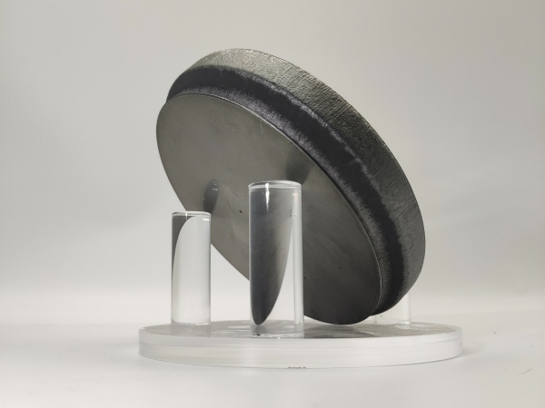
Si-on-SiC (silicon-on-silicon carbide) substrates address this limitation by integrating a thin single-crystal silicon device layer onto a semi-insulating 4H-SiC handle wafer via wafer bonding. This heterogeneous platform retains the mature manufacturing infrastructure of silicon device processing while leveraging the exceptional thermal properties and semi-insulating isolation of 4H-SiC. From a substrate supplier's perspective, this article reviews the fabrication processes, process yield, critical interfacial characteristics, and remaining material challenges associated with Si-on-SiC bonded substrates.
1. Structural Architecture of Si-on-SiC Substrates
The Si-on-SiC stack comprises two principal components:
- Handle Substrate: Semi-insulating 4H-SiC wafer (100 mm diameter, resistivity ≥ 1×10⁷ Ω·cm), which provides heat spreading, electrical isolation, and radiation hardness — serving as the mechanical and functional foundation of the stack.
- Device Layer: Thin n-type silicon film (1 μm or 2 μm nominal thickness), upon which lateral power devices such as LDMOS and IGBTs are subsequently fabricated.
| Key principle: Rather than epitaxially depositing silicon on SiC, this technology utilizes wafer bonding to transfer a silicon device layer from a starting SOI wafer onto the SiC handle. The original silicon handle and buried oxide (BOX) layer of the SOI wafer are then removed, yielding a direct Si/SiC bonded interface. |
 Figure 1. Schematic cross-section of the Si-on-SiC substrate stack and a lateral MOSFET device fabricated on the thin silicon device layer.
2. Comparison of Two 100 mm Si-on-SiC Bonding Processes
Both process flows begin with 100 mm semi-insulating 4H-SiC substrates and commercial SOI wafers as starting materials, and converge on a final Si-on-SiC bonded substrate structure. The two routes represent distinct technological paradigms for bonded substrate manufacturing.
2.1 BP1: High-Temperature Hydrophobic Bonding
Process sequence:
- Trench arrays are pre-etched into the SiC surface to outgas volatiles generated during high-temperature annealing.
- Both wafer surfaces undergo plasma-activated hydrophobic treatment, followed by room-temperature pre-bonding.
- Permanent bonding is achieved through a 2-hour anneal at 1200 °C.
- The SOI silicon handle is ground away, and the buried oxide (BOX) layer is removed by HF wet etching to reveal the final Si-on-SiC substrate.
Substrate-level limitations:The high-temperature annealing step induces significant wafer bow and residual mechanical stress. The interfacial oxide layer at the Si/SiC bonded interface is non-uniform, ranging from 0 to 2 nm in thickness, and contains a high density of interfacial defects and fixed charges. As a consequence, the
n-type silicon device layer exhibits an effective p-type inversion in electrical characterization — a severe drawback for device-to-device uniformity and high-volume manufacturing.
2.2 BP2: Low-Temperature Nitrogen-Radical-Activated Hydrophilic Bonding (Optimized Route)
Process sequence:
- Both the semi-insulating 4H-SiC substrates and SOI wafers undergo standard RCA cleaning, augmented by megasonic agitation.
- Wafer surfaces are activated in-situ with nitrogen radicals, achieving temporary hydrophilic bonding at room temperature.
- Permanent bonding is completed via a low-temperature anneal at only 300 °C for 24 hours under N₂ ambient, thereby eliminating the need for the 1200 °C high-temperature step.
- The SOI handle wafer is ground and removed, and the BOX layer is stripped with HF. The silicon device layer can subsequently be precisely thinned to the target thickness (1 μm) by dry etching.
Key performance metrics — critical for commercial-grade substrates:
- ✅ Bonding yield of 97% across full 100 mm wafers
- ✅ Void-free bonded interface; TEM reveals a uniform 1.4–1.8 nm thin interfacial oxide layer
- ✅ Bond strength exceeding 360 N (at the upper limit of the tensile tester), confirming robust mechanical reliability
-
| Experimental note: Post-bond annealing at 1150 °C was found to only marginally thin the interfacial oxide (by 7–9%), with negligible benefit. Consequently, the thin interfacial oxide layer is retained as-is, without additional high-temperature treatment. |
 Figure 2. TEM micrograph of the Si/SiC bonded interface obtained via the BP2 low-temperature process.
3. Impact of Device-Layer Thickness on Electrical Performance
For nominally identical
Si-on-SiC bonded substrates, the thickness of the silicon device layer has a pronounced effect on the resulting electrical behavior:
- 2 μm silicon device layer: Even with the optimized BP2 bonding process, the silicon film still exhibits p-type characteristics accompanied by significant frequency dispersion.
- Silicon layer thinned to 1 μm: Electrical properties revert toward the intended n-type behavior; however, residual frequency dispersion and incomplete charge accumulation persist.
| Substrate engineering insight: The 2 μm silicon layer retains the damaged region inherited from the original Si/BOX interface of the starting SOI wafer. Dry-etch thinning down to 1 μm removes this process-induced damage layer, substantially improving the electrical quality of the silicon film. This finding has direct implications for substrate specification: the choice of device-layer thickness is a critical design parameter that governs the overall electrical quality of the bonded substrate. |
4. Concluding Remarks
Si-on-SiC is a heterogeneous bonded substrate platform built upon semi-insulating 4H-SiC handle wafers, in which a thin silicon film is transferred via wafer bonding technology.
Low-temperature radical-activated bonding successfully addresses the key manufacturing challenges for large-area (100 mm) substrates — bonding voids, yield, and mechanical strength. Nevertheless,
interfacial trap charges at the Si/SiC bonded interface remain the principal technical bottleneck for this material system. Even for visually void-free, high-yield substrates, interfacial trap charges can still distort the electrical behavior of the overlying silicon device layer. Furthermore, device-layer thickness selection exerts a direct and significant influence on the overall electrical characteristics of the substrate.
About JXTJXT specializes in the development, manufacturing, and global supply of high-quality semiconductor substrate wafers. Our product portfolio includes silicon polished wafers, semi-insulating and conductive 4H-SiC substrates, and we offer custom wafer-bonding services for both heterogeneous and homogeneous bonding configurations — including Si/SiC, Si/SiO₂, and SiC/SiC — with wafer sizes ranging from 2-inch to 8-inch to meet diverse customer requirements. |